
4 Layer PCB Enhance Electromagnetic Compatibility EMC
A 4 layer circuit board is a circuit board with multiple copper layers that are instrumental in routing electrical signals efficiently. They can also be used for various electronic components and are often found in complex devices. When it comes to electromagnetic compatibility EMC, a 4 layer PCB offers better signal integrity, reduced noise, and improved performance than 2-layer boards.
Having the ground layer and power plane on outer layers minimizes radiated emissions. It is important to keep signal layers close to each other as well, in order to reduce signal-to-ground interference. The use of solid power and ground planes can also enhance the quality of the signals on the traces.
In a multi-layer stackup, the layers that are between the signal and power planes are responsible for the distribution impedance. The core and PP (prepreg) thickness is what controls this, and a thinner core and PP will result in a lower distribution impedance. The underlying copper of the signal layers should be sized to match the impedance of the power and ground planes. This can be achieved by using a thinner dielectric layer on the signal layers.
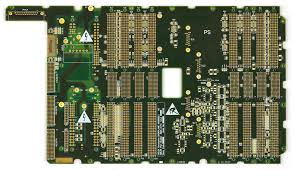
How Does a 4 Layer PCB Enhance Electromagnetic Compatibility EMC?
Another method to improve EMI performance is by using a Faraday cage around the board. This will protect the signal from external interference and also limit the field strength of the internal signals to a certain extent. It is a good idea to implement this mechanism whenever possible, as it will help you pass the EMC tests easily.
There are a lot of issues that can cause EMI problems in the design of electronic devices, and they all need to be addressed at different levels. Some of these may be related to the design process itself, while others might be related to the choice of components and their placement on the PCB. However, the most common problem that causes EMI issues in EMC testing is due to the PCB itself. Many of these issues can be resolved easily, and if you follow the advice given in this article and in other articles on our blog, you will be much more likely to pass the EMC test.
The PCB is a key component in all electronic devices, and it plays a major role in the overall functionality of the device. It is therefore crucial to make sure that the PCB is designed correctly, so that it can meet all of the requirements of the EMC tests and also perform at a high level in other ways. If you have any questions about EMC testing, please don’t hesitate to contact us, and we will be happy to help! We also invite you to check out our podcasts, where we interview the best engineers in the industry. This will give you a much better understanding of the subject and how to design your next circuit board. The experts on our podcasts have all told us that the PCB is one of the main sources of EMI problems in electronics, and they have all shared some valuable tips for how to avoid these problems.


