
Micro Vias Be Filled Or Plated
Vias are holes in a printed circuit board (PCB) that are used to transmit thermal and electrical signals. PCB manufacturers use different methods to create vias, including mechanical drills and laser beams. The type of drilling method and the design of the PCB’s stack-up can have a significant impact on the reliability of the vias and their ability to conduct thermal and electrical signals.
Depending on the layout of the PCB, the vias can be filled or plated. Filling the vias prevents solder and contaminants from entering the hole and prevents the formation of voids in the hole barrel. The process also increases the thermal transfer capabilities of the vias, allowing more heat to be dissipated from the components on the other side of the board.
Filling the micro vias is usually done with a non-conductive epoxy. This is useful for keeping solder or other contaminants from contaminating the via and it can also provide structural support for the copper pad in a blind microvia or a via-in-pad configuration. It is also possible to have a conductive fill in the vias, but this can increase the cost of the PCB.
Conductive via fills have a very high conductivity and they can easily transfer thermal energy from the IC to the copper pads on the other side of the board. This can be helpful in reducing the temperature of the IC and improving the overall performance of the device. However, if the vias are not correctly designed or placed on the device, they may become sources of failure.
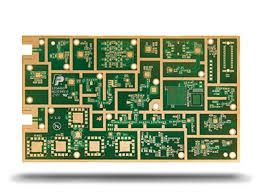
Can Micro Vias Be Filled Or Plated?
The manufacturing process for a PCB that has been designed with vias starts with cleaning and prep of the entire surface. The holes are then drilled with either a mechanical drill or a laser beam, depending on the layout of the PCB. The drilled holes are then cleaned using a combination of abrasive mechanical and chemical processes. This removes any debris that is left behind in the holes, such as burrs or resin residue.
Afterwards, the hole barrels are filled with copper. This can be done in several ways, such as through the use of photoresist that has been developed to expose only the areas of the via that require plating. Then the vias are plated with pure copper or an epoxy +copper resin. Plating processes that do not incorporate some additive in the filler material can lead to void formation in the body of the via. Conformal plating can also contribute to uneven deposition of copper along the via body, resulting in voids.
The best way to reduce the chance of voids and other issues with your vias is to plan properly in the CAD software. For example, when defining the layer pairs for the vias in your PCB, make sure that you are using the appropriate via sizes and that you have an adequate annular ring around the entire hole. It is also important to work closely with your PCB fabricator to ensure that the gerber files that you submit for fabrication are correct.


