
HDI PCB Enable Miniaturization
The increasing trend towards miniaturization of electronic devices has created a challenge for the PCBs that hold and connect these components. The development of high-density interconnect (HDI) technology enables designers to develop compact boards with higher performance, reliability, and functionality while reducing the size of their final product.
A key component of hdi pcb is the use of blind and buried vias, which are smaller holes that enable higher density routing within a small footprint. This increased routing density translates into more features on a single PCB, reduced power and signal transmission delays, and lower cross-talk between signals. The combination of these features leads to lighter, more compact, and lower-cost PCBs.
HDI PCBs can be fabricated using two different structure types: build-up/sequential laminations and any-layer structures. In build-up/sequential lamination, cores are constructed, laminated, drilled, and plated in stages. These phases are repeated for each layer. This technique enables manufacturers to achieve higher layer count manufacturing while maintaining the integrity of the copper-filled microvias.
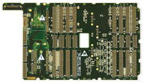
How Does HDI PCB Enable Miniaturization?
In an any-layer structure, every layer is a high-density interconnection layer. Conductors on any layer can be freely interconnected with copper-filled stacked microvias structures, which provides a reliable interconnect solution for large pin-count devices such as CPU and GPU chips utilized in handheld and mobile devices while producing superior electrical characteristics. The any-layer HDI PCB is an ideal solution for achieving the compact form factor and high performance required in the latest handheld and mobile devices.
Another advantage of the HDI PCB is its ability to be etched using laser drilling techniques. Laser-drilled holes are less prone to warping and cracking and provide better thermal properties than conventional mechanically drilled holes. Laser-drilled holes also allow for a faster and more accurate process, which reduces manufacturing time and costs.
As the demand for more compact and functional electronics grows, more manufacturers are offering HDI PCBs as a way to meet these demands. However, there are several important factors to consider when choosing a manufacturer for your project. First, you should determine the manufacturer’s lead times and production capacity to ensure they can meet your deadlines. Next, you should make sure the manufacturer has a proven track record of quality and adhering to industry standards. Finally, you should review the technical documents and prototypes produced by the manufacturer to ensure the quality of their work.
The high-density interconnects of HDI PCBs require special consideration during the design process to maintain signal integrity, power distribution, and thermal management. Specialized expertise and advanced tools are needed to manage these challenges. In addition, it is critical to follow DFM guidelines and simulation tools to ensure manufacturability and quality. Finally, a thorough review of the Gerber files is essential to prevent errors during production. By following these tips, you can ensure that your HDI PCB will deliver the performance and reliability your customers expect.


